石墨烯纳米带制备研究获新进展 |
|
|
| 来源:《先进材料》 更新时间:2011-4-22 11:01:49 |
|
|
|
|

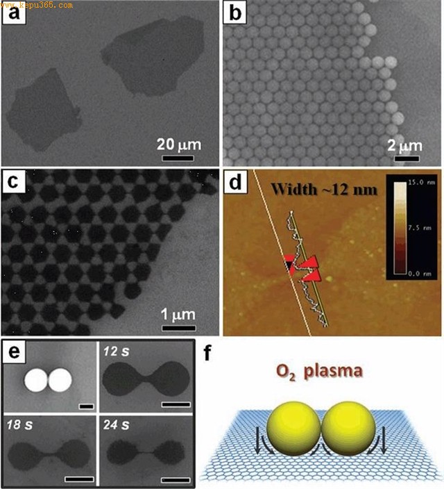
Figure 1. a) SEM image of the chemically derived graphene sheets lying on a SiO2/Si substrate. b) SEM image showing a domain of the hcp PS nanosphere monolayer that masked the graphene sheets. c) SEM image of the large area, interconnected 2D GNRs network etched through an hcp monolayer NSL mask. d) Tapping mode AFM image of a selected typical nanoribbon with width of ca. 12 nm (measured via line scan profile). e) SEM images showing the temporal evolution of the individual dumbbell-like GNRs etched through the isolated pairs of packed nanospheres (top panel) with etching durations of 12 s, 18 s and 24 s. Scale bars in (e): 500 nm. f) Schematic illustration (not to scale) showing the NSL-defined lithographic etching process of graphene sheets.

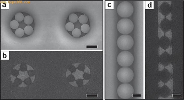
Figure 2. a, c) SEM images showing the well-defined nanosphere pentagons and linear chains formed from ≈ 1 μ m PS nanospheres in the ≈ 3 μ m cylindrical holes of the photoresist and 2 μm spheres in photoresist trenches with ≈ 2 μm width. b, d) SEM images of the pentagonal ring and linear chain architectures of connected GNRs, etched through the corresponding nanosphere masks. Scale bars: 1 μm.

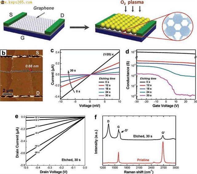
Figure 3. a) Schematic illustration of the on-chip bandgap tuning of graphene through NSL nanopatterning and subsequent O2-plasma etching. b) AFM image of a typical FET device based on the mechanically cleaved single-layer graphene sheet. [1] [2] 下一页
|
上一篇科学技术: 科学家发明依靠光照自我修复新型塑料
下一篇科学技术: 科学家利用果蝇编织出天然纤维 |
|
|
|
|
|
|
